Category: Homemade CPU

BizzasCPU springs to life v2.0

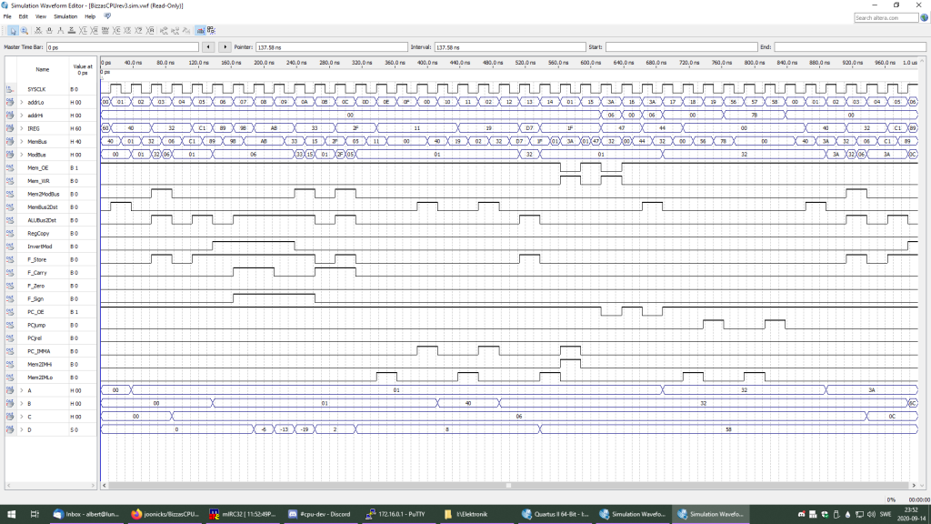
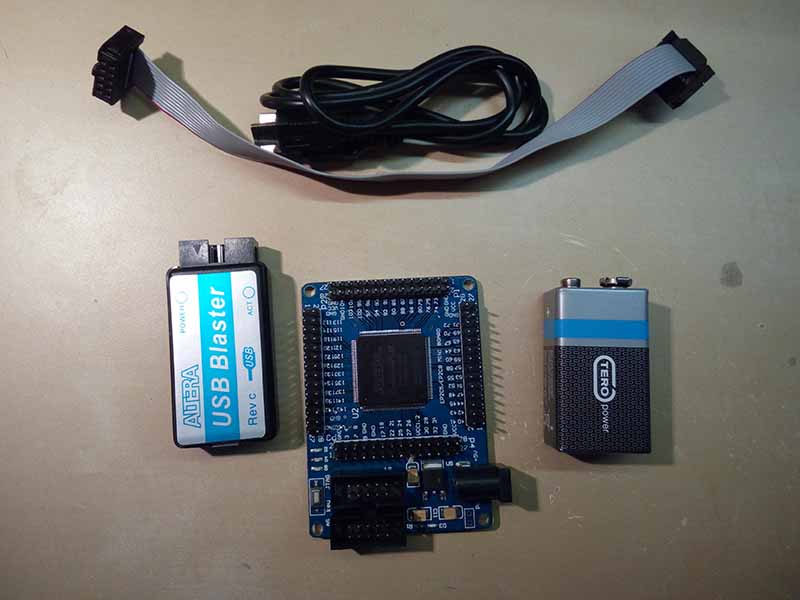
After two years of developing and simulating, BizzasCPU today took the step into actual hardware. The first ever upload into an actual FPGA started the parade of blinking LEDs and established that it works quite well. In fact the first run was so fast that it needed to be slowed down by a factor of 10,000 to be able to verify without a doubt that it is fully functional and operates as expected.

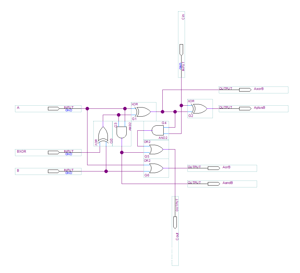
The host FPGA was a Terasic DE10-Nano development board and the operating frequency was 12.5MHz. The frequency however can most likely be bumped up significantly, if needed. The BizzasCPU design has much higher MIPS per Clock compared to a 6502 or Z80, but instruction complexity is somewhere inbetween, being more versatile than 6502, but less than a Z80.

Now follows the need for a proper assembler and more IO to make it more fun to play around with. Just 8 LEDs blinking is not the most inspiring.

Of course it will now be fun to run around bragging about my very own CPU design. Future will tell if anyone ever notices.

BizzasCPU springs to life

Around the beginning of September, I resumed work on my old CPU project that had been collecting dust on github. After about 10 days work, I reached a point where I started implementing the logic for instruction execution.

The more simple instructions were all added and verified quite quickly. Last ones to be implemented were JMP and memory access instructions. JMP instructions actually turned out to be extraordinarily simple logic.

It currently compiles into less than 300 logic elements, so it is a very simple (8-bit data, 16-bit address) CPU design.

Here is what it looks like running in simulation software:

It still hasnt been tested on FPGA hardware, hopefully that day will come before more years pass. I just ordered a Terasic DE10-Nano which has more test hardware built onto it, which should make debugging easier.

For more details on BizzasCPU, check out the github repository: https://github.com/joonicks/BizzasCPU

The beginning…

A couple of weeks back I started designing my own CPU (called Bizzas CPU) in Quartus II with the initial goal of getting it running on an FPGA. Right now im bouncing between many different tasks as well as trying to just chillax from time to time.

Elements of a CPU such as registers, program counters and ALU‘s are pretty easy to design. I have most of that done. My current task is to design a robust and efficient instruction decoder, or instruction executor as I call it. After that, I will make an instruction loader.

Once those are done, the CPU will hopefully be ready to run inside the FPGA without any significant connections to the outside world. Then the next step is to wire it up to some memory and other peripherals, maybe even make a VGA interface.

End goal is ofcourse world domination!

Here is what a 1-bit ALU block looks like inside:

alu1bit

This particular configuration can do add, subtract, XOR, AND and OR. Not bad for only 7 logic gates.

My project is shared in its entirety on GitHub: https://github.com/joonicks/BizzasCPU

FPGA arrived

Just arrived from China, a small cheap FPGA: Altera Cyclone-II (EP2C5T144).

The device itself is the least capable of all the Cyclone II FPGAs, but its seriously cheap at only $13. And its big enough to hold a basic CPU core. This is what it looks like (9V battery included for scale):

FPGA1

The USB Blaster has to be bought separately but only costs an additional $3. Unfortunatly the DC jack is for 5V, its unregulated unlike Arduinos. Bummer. And I dont have any 5V adapter with a 5.5mm plug so I have to make one myself.

Here are the specs for the board itself (and others of the same family, its the smallest one, EP2C5):

cyclone_specs

So now Im mostly ready to start designing and testing my own CPU. Ive already started some basic designing since a couple of nights back. Gaining some insights and making early design choices.

I still havent committed to wether the data bus should be 8-bit or 16-bit. Id like to make it 16-bit but that means a whole lot of wires (since its ultimately imagined as a breadboard design). Now that I think of it maybe I should make a first test design with address bus and data bus both being 8-bit.